Paparan:1 创始人: Site Editor Publish Time: 2024-11-20 Origin: Site


SMT processing and manufacturing involves
many links, from the basic concept of PCB, to the difference between SMT and
THT processes, to the analysis and solution of quality problems in various
soldering processes.
1.
SMT is related to the THT process
· PCB is an important support and electrical connection provider of
electronic components, and the SMT process is fundamentally different from the
traditional THT process in terms of assembly technology, which is reflected in
"pasting" and "plugging". THT uses leaded components, and
the SMT circuit board assembly density is greatly increased by inserting the
component leads into the PCB through holes and soldering on the other side of
the substrate, while the SMT solder joints are on the same side of the board as
the components. DIP packaging is one of the THT plug-in processes, and the
trend of high-performance computing packaging is shifting from FCBGA and 2.5D
packaging to 3D packaging, and electronic components are redesigned to SMDs
that can be soldered directly to PCBs or other substrate surfaces.
2.
SMT dispensing process defects and solutions
· In the SMT dispensing process, there are common defects such as
component displacement, wafer drop after wave soldering, and
floating/displacement of component pins after curing.
· The causes of component displacement include uneven amount of
adhesive output from the SMT, component displacement or low initial adhesion
during SMT, and long PCB placement time, etc., and the solution is to check the
nozzle, adjust the placement machine, change the glue, and control the PCB
placement time.
· Falling off after wave soldering is due to insufficient curing
process parameters, large component size, aging of curing lamps, insufficient
glue volume, contamination of components/PCBs, etc., which can be solved by
adjusting the curing curve, checking the curing lamp, and considering the
amount of glue and component/PCB contamination.
· After curing, the floating/displacement of the component pins is caused by uneven placement adhesive, excessive amount, or component deviation during placement, and the solution is to adjust the dispensing and placement process parameters.

3.
Solder paste printing quality
· Poor printing of solder paste will lead to a variety of quality
problems, such as insufficient paste solder will cause insufficient amount of
solder in solder joints, open circuits of components, etc.; Adhesion can lead
to short-circuits, etc.; The overall deviation of printing leads to poor
welding of the whole board components; Pulling the tip can cause a short
circuit.
· There are many factors that lead to the shortage of solder paste,
including the printing press does not replenish the solder paste in time, the
quality of the solder paste is abnormal, the expired use, the circuit board is
problematic, the fixed clamp is loose, the problem of missing the printing
screen, the scraper and the screen plate are damaged, the equipment parameter
setting is not appropriate, and the artificial touch is removed.
· The main factors of solder paste adhesion are circuit board design
defects, stencil problems, failure to wipe clean, poor solder paste
performance, loose fixing and clamping, inappropriate equipment parameter
settings, artificial extrusion and adhesion, etc.
· The main factors of the overall deviation of solder paste printing
are the problem of the positioning reference point of the circuit board, the
misalignment with the reference point of the screen board, the loose fixing
clamp, the lack of positioning thimble, the failure of the optical positioning
system of the printing machine, and the inconsistency between the opening of
the screen and the design documents.
· The main factors of printing solder paste are solder paste
performance parameter problems, demoulding parameter setting problems, and
burrs on the hole wall of the missing printing screen plate.
4.
SMT patch quality is related
· The common quality problems of SMT patch include missing parts, side
parts, turning parts, deviations, damaged parts, etc.
· The factors that lead to missing parts include insufficient feeding
of component feeding racks, component nozzle problems, equipment gas circuit
failures, poor circuit board purchases, solder paste problems on pads,
component quality problems, placement machine program errors and omissions,
etc.
· The main factors of turning parts and side parts during SMC resistor
placement are abnormal feeding of the feeding rack, wrong nozzle height, wrong
grasping height, too large size of the component taping charging hole, and
reverse direction of bulk material.
· The misalignment of the component is due to the incorrect
coordinates of the placement machine and the unstable suction of the chip
nozzle when the placement machine is programmed.
· The damage during component placement is caused by the positioning
of the ejector pin is too high, the Z-axis coordinate is incorrect when the
placement machine is programmed, and the nozzle spring is stuck.
5.
Factors that affect the quality of SMT reflow soldering
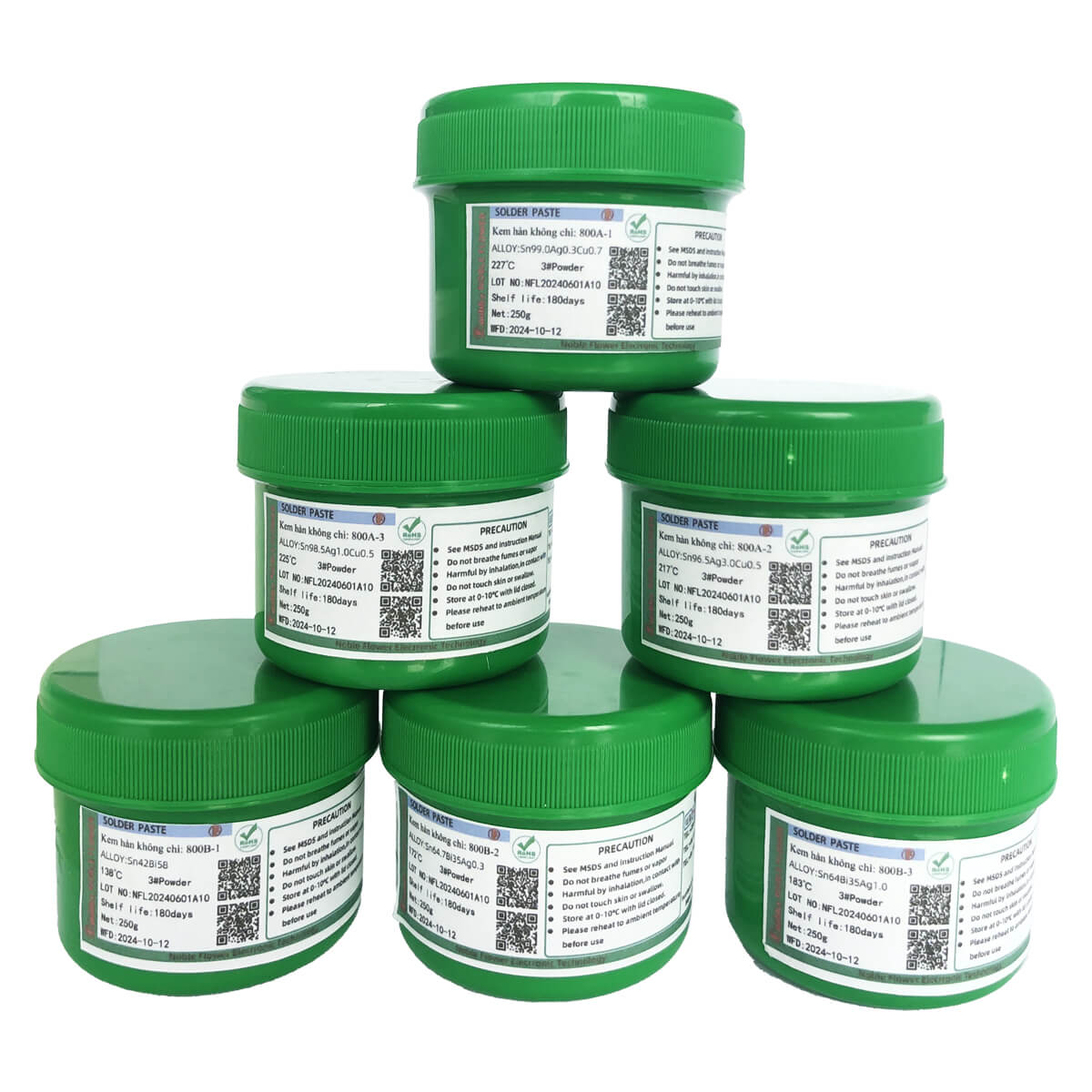
· In terms of solder paste, the quality of reflow soldering is greatly
affected, such as the shape of alloy powder particles is related to the welding
quality of narrow-pitch devices, the viscosity and composition should be
appropriate, and the use specification after refrigerated storage should be
paid attention to.
· In terms of welding equipment, the vibration of the conveyor belt of
reflow soldering equipment is too large, which affects the welding quality.
· The reflow soldering process itself will lead to quality
abnormalities such as cold welding, solder beads, tinning, cracks, etc., each
with its own corresponding causes and solutions.
· The fundamental cause is the unbalanced wetting force on both sides
of the component, which is related to the design and layout of the pad, solderpaste and printing, chip displacement, furnace temperature curve, oxygen
concentration in nitrogen reflow soldering and other factors, and there are
corresponding solutions.
· Solder beads can be divided into two categories, and the causes
include incorrect temperature profiles, solder paste quality problems, printing
and placement problems, etc., and solutions are also given for these reasons.
· The wicking phenomenon is mostly seen in vapor phase reflow
soldering, which is mainly caused by the high thermal conductivity of component
pins, and the solutions include preheating, checking the solderability of PCB
pads, and paying attention to component coplanarity.
· Bridging can cause short circuits in components due to solder paste quality problems, printing system problems, excessive placement pressure, and rapid heating up of reflow ovens.

6.
Wave soldering quality defects and solutions
· Drawing the tip is a defect unique to wave soldering, and the cause
is related to the PCB transfer speed, preheating temperature, tin pot
temperature, etc., and the solution is to adjust the relevant parameters,
optimize the nozzle, etc.
· The causes of virtual soldering include a variety of factors such as
poor solderability of component leads, and the solution is to adjust these
factors.
· The cause of tin thinness is related to the solderability of
component leads, pad size, etc., and there are corresponding solutions.
· The causes and solutions of missing soldering are also given
according to the solderability of the leads, wave device, flux, etc.
· The fundamental reason for the blistering of the solder mask film of
the printed board after welding is the presence of gas or water vapor between
the solder mask mold and the PCB substrate, which is related to the PCB
processing process, storage environment, preheating temperature and other
factors.
· The reasons for open circuit or virtual soldering after IC pin
soldering include poor coplanarity, poor pin solderability, poor paste solder
quality, high preheating temperature, small printing template window size,
etc., the solution is to pay attention to device storage, check solderability,
control template window size, etc.
To sum up, the quality problems of SMT
processing and manufacturing and welding are complex and diverse, and it is
necessary to strictly control each link, accurately analyze the causes of
different quality problems and take effective solutions to ensure the quality
of SMT processing and manufacturing.
 Su Gongwang Security 32058302004438